RTT News, Business Weekly, Optics.org, Electronics Weekly: e2v is to acquire Seville, Spain-based Innovaciones Microelectronicas SL, also known as AnaFocus for up to 34.2M euros.
The initial cash purchase price of 29.2M euros is made up of 26.5M euros cash consideration for the business, and assumed net debt of 2.7M euros. The AnaFocus management team is staying with the business and can achieve an earn-out of up to 5M euros in cash, dependent on value generating 'stretch' integration targets including revenue growth. In 2013, AnaFocus had revenues of 5.6M euros and EBITA of €80,000. In the calendar year to December 31, 2014 AnaFocus is expected to generate sales of approximately €11M.
e2v technologies’ Group CEO, Steve Blair, said: "AnaFocus adds technology, people and customers to our machine vision business. It strengthens our position in the market, bringing to e2v a successful management team with deep technology capabilities and close relationships with customers that complement e2v’s relationships. The strength of the AnaFocus team, and the e2v worldwide sales and customer support channels they can now access, will help us to accelerate our opportunities in this fast-growing business. We see immediate opportunities to apply the technical capabilities of AnaFocus to provide enhanced offerings to our joint customers. I am delighted we are making this acquisition and I am pleased the AnaFocus team are joining us."
e2v expects the acquisition to complete during September 2014. AnaFocus will become an integral part of the machine vision business within e2v’s High Performance Imaging division, which grew by 26% last year. Both e2v and Anafocus use TowerJazz as their sole foundry partner for CMOS image sensors.
Aptina Completes CFA Fab Acquisition
Business Wire: Aptina has completed the purchase of CFA processing and imager probe assets from Micron. Following the purchase, Aptina will operate a fabrication facility in Nampa, Idaho that employs nearly 100 employees who will work closely with Aptina’s existing pixel optics research and development team. In addition, Aptina will hire management, development and support roles to bring its Idaho presence to approximately 250 total employees.
Sony Reports CMOS Sensor Sales Growth, Updates Yearly Targets
Sony posts its quarterly results and reports a significant image sensor sales increase and a camera module production launch:

Sony also has updated its semiconductor business flyer, increasing FY2014 image sensor sales target to 390B yen, up from 360B yen in the previous flyer from 2 months ago. The CMOS sensor production capacity increased from 60M units per month to 75M units, and the planned capital investment in image sensors rises from 450B to 500B yen:

Sony also has updated its semiconductor business flyer, increasing FY2014 image sensor sales target to 390B yen, up from 360B yen in the previous flyer from 2 months ago. The CMOS sensor production capacity increased from 60M units per month to 75M units, and the planned capital investment in image sensors rises from 450B to 500B yen:
Samsung Files for Lightfield Imager Patent
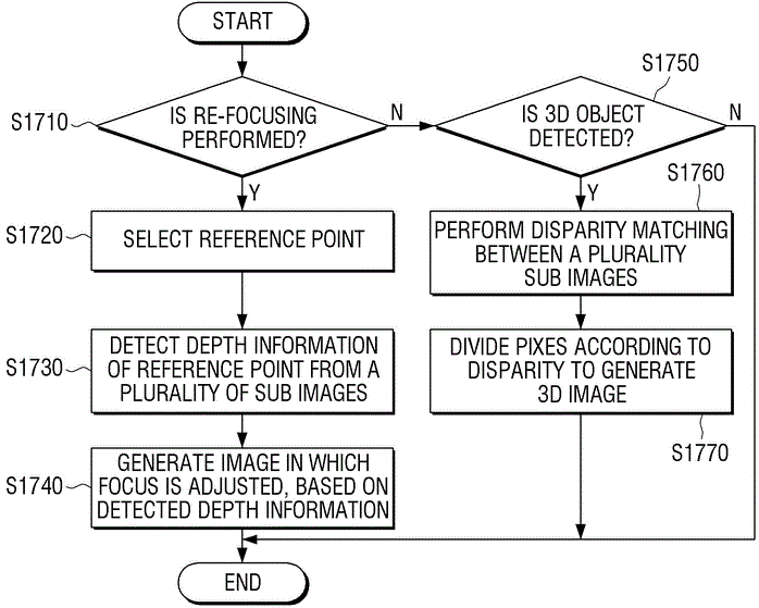
Samsung patent application US20140204183 "Photographing device and photographing method for taking picture by using a plurality of microlenses" by Tae-Hee Lee, Stepan Tuliakov, Hee-chul Han proposes to move color filter in front of big microlenses in order to avoid demosaicing blur in each sub-image:


Cambridge Mechatronics Announces First OIS Customer
Cambridge Mechatronics Ltd. (CML) announces that the first customer for its smart metal alloy (SMA) OIS actuators is Foxconn. In a separate announcement, CML names its manufacturing partner, Hutchinson Technology Inc. (HTI). CML and HTI have been developing OIS actuators in collaboration with Foxconn's camera division for over 18 months. Following design wins in May, smartphones with cameras built by Foxconn using SMA OIS actuators will reach the market in September this year.
In June, CML announced that it will be making its OIS actuators for 1/3" to 1/2.3" image sensors with up to 20MP resolution.
The OIS actuator is attached between the image sensor and AutoFocus actuator. The motion of the OIS actuator moves the lens relative to the image sensor, counteracting any shake measured by a gyroscope and thereby stabilizing the image. CML's OIS actuators force and motion are created by Shape Memory Alloy (SMA) wire - a smart material that provides huge force and strain when heated with an electric current. CML says it is able to make smaller and lower cost products than VCM manufacturers.
Workshop on CMOS Active Pixel Sensors for Particle Tracking
University of Bonn, Germany conducts Workshop on CMOS Active Pixel Sensors for Particle Tracking (CPIX14) on Sep. 15-17, 2014. Although the workshop is fully booked, the organizers offer a live broadcast over the Internet for the presenters who agree - the world's first for an image sensor event.
The workshop's agenda:
Technology and design I
The workshop's agenda:
Technology and design I
- Overview Technology Offers
Tomasz Hemperek (Universitaet Bonn (DE)) - Design and process development of CMOS image sensors with TowerJazz
Renato Turchetta (STFC - Rutherford Appleton Lab. (GB)) - APSEL Deep n-well and Deep p-well CMOS Sensors with ST and TowerJazz Technologies
Gianluca Traversi (University of Bergamo)
- Deep n-well CMOS Sensors with 3D Integration of Global Foundries Wafers
Valerio Re (INFN) - DMAPS Design in XFAB Technology
Tetsuichi Kishishita (University of Bonn) - Development of DMAPS Sensors in ESPROS Technology
Miroslav Havranek (Acad. of Sciences of the Czech Rep. (CZ))
- ESPROS technology
Martin Popp (Espros Photonics) - LFoundry Technology
Gerhard Spitzelsperger (LFoundry) - TowerJazz Technology
Avi Strum (TowerJazz)
- Design detail and performance of Fully Depleted Backside Illuminated CMOS Sensors
Stefan Lauxtermann (Sensor Creations) - AMS High Performance CIS Modules
Ingrid JONAK-AUER (AMS) - Rad-hard design in CMOS [image] sensors
Bart Dierickx (Caeleste) - Image Sensor Design and Technology Development at Fraunhofer IMS
Sasha WEYERS (Fraunhofer IMS)
- PERCIVAL: CMOS Image Sensors for Low Energy X-Ray Detection
Iain Sedgwick (STFC) - AMS Designs: CLICPix/CCPD/Mu3e
Ivan Peric (Ruprecht-Karls-Universitaet Heidelberg (DE)) - CCPD Design: from AMS to GF technology
M. Patrick Pangaud (Centre National de la Recherche Scientifique (FR))
- Design of CMOS Pixels Sensor for the STAR Experiment
Christine Hu (IPHC/IN2P3) - STAR MAPS Developments and Experiences
Leo Greiner (Lawrence Berkeley National Laboratory) - Alice Designs: Mistral, Astral, Alpide
Marc Winter (Institut Pluridisciplinaire Hubert Curien (FR))
- CMOS pixels for electron microscopy: requirements and R&D results at TEAM
Marco Battaglia (University of California,Santa Cruz (US)) - Radiation hard MAPS developments for electron microscopy
Peter Denes (LBNL) - CMOS APS for TEM
Nicola Carlo Guerrini (STFC - RAL)
- MAPS are for amateurs, professionals do 3D
Grzegorz Deptuch (Fermi National Accelerator Lab. (US)) - Advances in Bonding technologies (chip to wafer and wafer to wafer)
Ray Yarema (FNAL)
- Experience with IBM 130 nm Process for Active CMOS Pixels
Dario Gnani (LBNL) - Fully depleted MAPS: Pegasus and Mimosa 33
Maciej KACHEL (IPHC) - SLAC Developments in CMOS Sensors
Julie Segal (SLAC)
- X-ray image sensors for SACLA and future Ultimate Storage Ring Light Sources
Nobukazu Teranishi (University of Hyogo) - Lapis SOI Technology and Designs
Yasuo Arai (High Energy Accelerator Research Organization (JP))
- Characterization of CCPDV3 HV-CMOS sensors capacitively coupled to CLICpix 65 nm CMOS readout ASICs
Mathieu Benoit (CERN LCD) - CMOS MAPS in Planar and 3D Technologies: TID Effects and Bulk Damage Study
Lodovico Ratti (University of Pavia) - Radiation Hardness of the Tower/Jazz 0.18 µm Imaging CMOS Process
Michael Deveaux (Johann-Wolfgang-Goethe Univ. (DE))
- Design and Characterization of a High-Speed Multi-frame Hybrid CMOS Sensor
John Porter (Sandia National Laboratories) - ESPROS DMAPS: Results and Radiation Hardness
Theresa Obermann (Universitaet Bonn (DE))
Mobileye IPO Values Company at $5.31B
Reuters: Mobileye's NYSE IPO on Aug. 1st values the vision-based ADAS company at about $5.31 billion, higher than planned. The company estimates that its products were installed in about 3.3M vehicles worldwide as of March 31, including BMW, Honda and Tesla Motors. By the end of 2014, it expects its technology to be available in 160 car models from 18 original equipment manufacturers worldwide.
Here is BMW TV story:
Update: The valuation has jumped to $7.86B in the first day of trade.
Here is BMW TV story:
Update: The valuation has jumped to $7.86B in the first day of trade.
Subscribe to:
Posts (Atom)